Applied Materials to boost semiconductor innovation with launch of its R&D platform in Silicon Valley
By MYBRANDBOOK
Applied Materials has announced a landmark investment to build the largest and most advanced facility for collaborative semiconductor process technology and manufacturing equipment research and development (R&D). The new Equipment and Process Innovation and Commercialization (EPIC) Center is planned as the heart of a high-velocity innovation platform designed to accelerate development and commercialization of the foundational technologies needed by the global semiconductor and computing industries.
To be located at an Applied campus in Silicon Valley, the multibillion-dollar facility is designed to provide a breadth and scale of capabilities that is unique in the industry, including more than 180,000 square feet – more than three American football fields – of state-of-the-art cleanroom for collaborative innovation with chipmakers, universities and ecosystem partners. Designed from the ground up to accelerate the pace of introducing new manufacturing innovations, the new EPIC Center is expected to reduce the time it takes the industry to bring a technology from concept to commercialization by several years, while simultaneously increasing the commercial success rate of new innovations and the return on R&D investments for the entire semiconductor ecosystem.
“While semiconductors are more critical to the global economy than ever before, the technology challenges our industry faces are becoming more complex,” said Gary Dickerson, President and CEO of Applied Materials. “This investment presents a golden opportunity to re-engineer the way the global industry collaborates to deliver the foundational semiconductor process and manufacturing technologies needed to sustain rapid improvements in energy-efficient, high-performance computing.”
Tremendous growth in the number of connected devices and the rise of artificial intelligence are driving increasing demand for chips and the opportunity for a $1 trillion semiconductor market. At the same time, chipmakers face significant challenges to sustain the pace of innovation required to meet this demand.
While these technology inflections continue to drive the industry forward, the sheer complexity of the engineering challenges requires a new approach to R&D. The traditional development model, starting with materials engineering equipment and process innovation, is a serial, compartmentalized process with no central hub for collaboration across the ecosystem. The industry needs a new model that breaks down traditional silos, builds denser networks of collaboration, and delivers tighter feedback loops that can increase the speed and lower the cost of innovation.
Applied’s new EPIC Center is designed to be a premier platform for leading logic and memory chipmakers to collaborate with the equipment ecosystem. For the first time, chipmakers can have their own dedicated space within an equipment supplier facility, extending their in-house pilot lines and providing early access to next-generation technologies and tools – months or even years before equivalent capabilities can be installed at their facilities.
The platform is also expected to be a catalyst for accelerating the commercialization of academic research and strengthening the pipeline of future semiconductor industry talent.
Universities are uniquely skilled at ideating new concepts, but they often lack access to state-of-the-art industrial labs and hardware which can impede their ability to turn ideas into commercial reality. Applied’s new platform can provide university researchers access to the full range of industrial-scale capabilities to validate their ideas, increasing the success rate of innovations and reducing the time and cost of commercializing new technologies.
To create the EPIC Center, Applied Materials expects to make gross, incremental capital investments of up to $4 billion over the next seven years. The new innovation center is expected to be completed by early 2026 and become the nexus of more than $25 billion in company R&D investments in the first 10 years of operations. The center is expected to employ up to 1,500 construction workers during the building period and create up to 2,000 new engineering jobs in Silicon Valley and potentially another 11,000 jobs in other industries.
EPIC is designed to be capable of engaging with a future U.S. National Semiconductor Technology Center. The scale of Applied’s investment is contingent upon receiving support from the U.S. government through provisions of the CHIPS and Science Act.


Legal Battle Over IT Act Intensifies Amid Musk’s India Plans
The outcome of the legal dispute between X Corp and the Indian government c...

Wipro inks 10-year deal with Phoenix Group's ReAssure UK worth
The agreement, executed through Wipro and its 100% subsidiary,...

Centre announces that DPDP Rules nearing Finalisation by April
The government seeks to refine the rules for robust data protection, ensuri...

Home Ministry cracks down on PoS agents in digital arrest scam
Digital arrest scams are a growing cybercrime where victims are coerced or ...

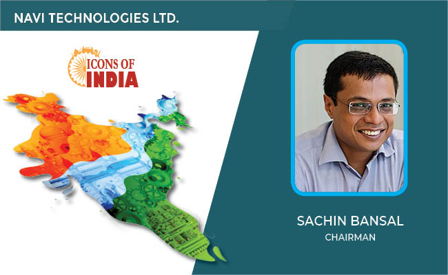
ICONS OF INDIA : SACHIN BANSAL
Sachin Bansal is an Indian entrepreneur. He is best known as the found...

Icons Of India : MADHABI PURI BUCH
Madhabi Puri Buch is the first-female chairperson of India’s markets...
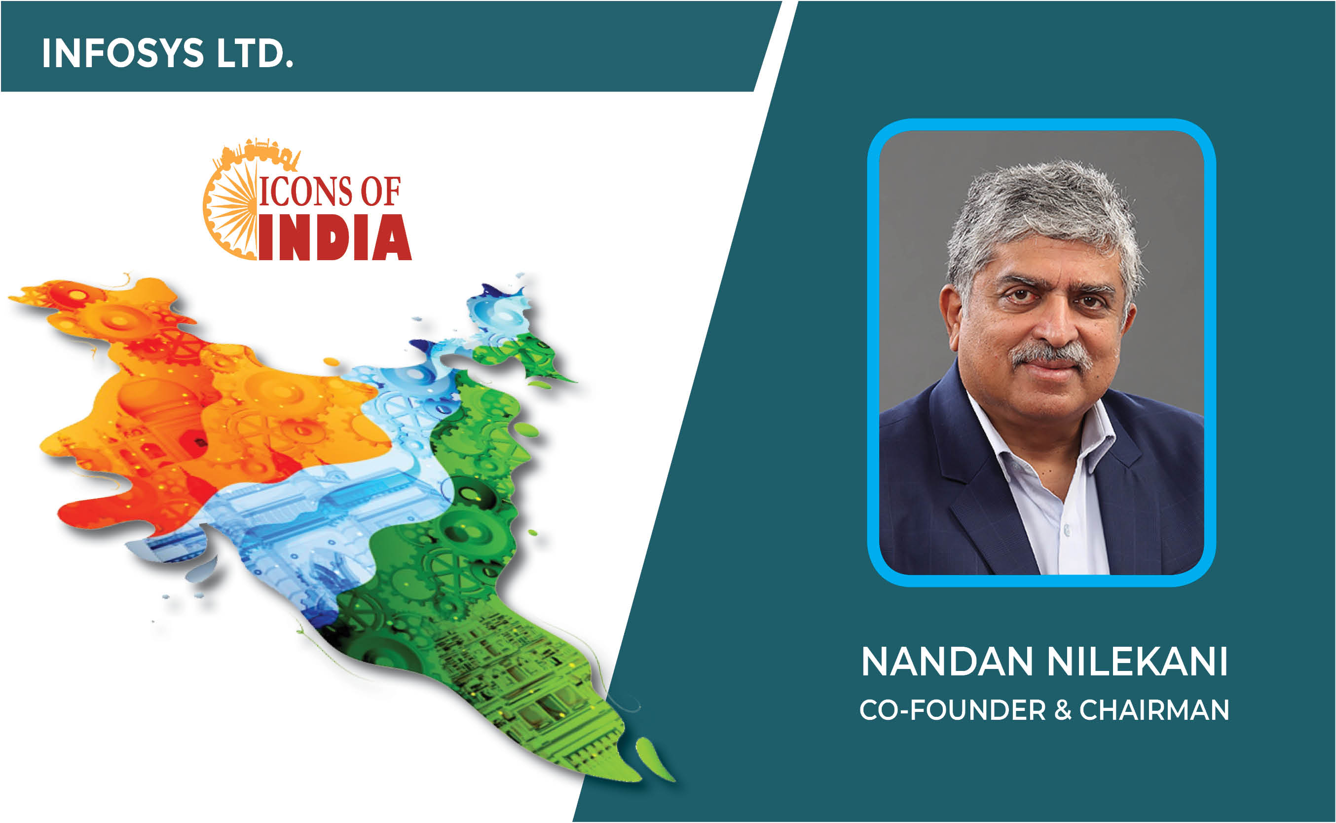
Icons Of India : NANDAN NILEKANI
Nandan Nilekani is the Co-Founder and Chairman of Infosys Technologies...

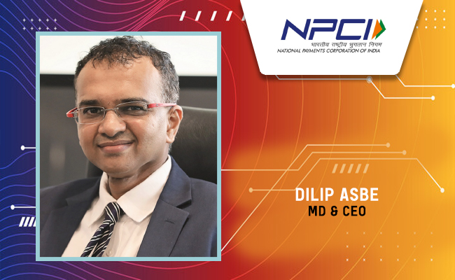
NPCI - National Payments Corporation of India
NPCI is an umbrella organization for operating retail payments and set...

IREDA - Indian Renewable Energy Development Agency Limited
IREDA is a specialized financial institution in India that facilitates...
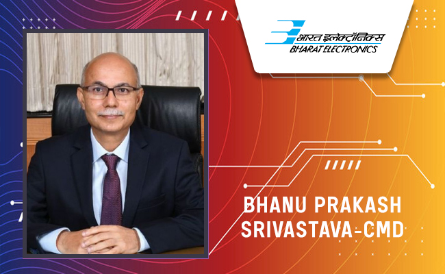
BEL - Bharat Electronics Limited
BEL is an Indian Government-owned aerospace and defence electronics co...


Indian Tech Talent Excelling The Tech World - REVATHI ADVAITHI, CEO- Flex
Revathi Advaithi, the CEO of Flex, is a dynamic leader driving growth ...

Indian Tech Talent Excelling The Tech World - Soni Jiandani, Co-Founder- Pensando Systems
Soni Jiandani, Co-Founder of Pensando Systems, is a tech visionary ren...

Indian Tech Talent Excelling The Tech World - AJAY BANGA, President - World Bank
Ajay Banga is an Indian-born American business executive who currently...
 of images belongs to the respective copyright holders